

Understanding Motherboard Diagrams
What is a Motherboard Diagram?
Imagine trying to assemble a high-tech Lego set without the instructions—that’s what tackling a motherboard without understanding its diagram is like. A motherboard ka diagram acts as a treasure map, guiding you through the labyrinth of ports, slots, and circuits that keep your PC humming along. It’s the blueprint that reveals where your CPU, RAM, and expansion cards should sit, making the complex world of motherboard ka diagram surprisingly approachable.
Understanding a motherboard ka diagram isn’t just for tech geeks; it’s essential for anyone wanting to troubleshoot or upgrade their system. It showcases everything from power connectors to SATA ports, helping you visualise how each component interacts. For example, knowing the exact location of the PCIe slots can make installing a new graphics card as smooth as butter. Without this visual aid, even the simplest upgrades can turn into a frustrating scavenger hunt.
Importance of Motherboard Diagrams in PC Building
Understanding a motherboard ka diagram is more than just a technical necessity; it is a window into the very soul of your PC’s architecture. When you grasp the layout, you unlock the potential to troubleshoot with precision and upgrade with confidence. The importance of a motherboard ka diagram lies in its ability to demystify the complex web of circuits, ports, and slots that define your system’s core. It transforms an intimidating maze into a comprehensible map, guiding your hand through the intricate process of assembly and maintenance.
For anyone venturing into PC building, recognising the significance of a motherboard ka diagram is essential. It reveals the precise locations of critical components—like the CPU socket, RAM slots, and power connectors—ensuring each piece fits seamlessly into the bigger picture. In fact, familiarity with this diagram can turn what might seem a daunting task into a smooth, almost intuitive experience. After all, when you understand the layout, you become the architect of your own digital universe, shaping it with insight and clarity.
Common Symbols and Icons Used
Delving into a motherboard ka diagram reveals an enchanting universe of symbols and icons, each whispering secrets about your system’s intricate design. These common symbols serve as a visual language, transforming complex circuitry into a decipherable map that guides even a novice through the labyrinth of components. For instance, a small square with a lightning bolt often signifies power connectors, while a cluster of tiny rectangles typically marks RAM slots, each symbol acting as a signpost on your journey of PC assembly.
Recognising these icons is akin to learning a new language—one that unlocks the true potential of your motherboard ka diagram. To make navigation smoother, many diagrams employ universally recognised symbols such as arrows indicating direction or colour-coded connectors for clarity. When familiarised with these visual cues, understanding the motherboard ka diagram becomes an intuitive process, transforming technical complexity into a delightful adventure of discovery and mastery.
Components Highlighted in Motherboard Diagrams
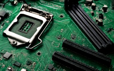
CPU Socket and Power Connectors
Within the intricate tapestry of a motherboard ka diagram, the CPU socket emerges as a vital nexus — a portal where processing prowess converges with the motherboard’s silent symphony. This socket, often a finely crafted square or rectangular frame, cradles the CPU, ensuring a seamless dance of electrical signals and data exchange. Its precise placement is crucial, as it anchors the heart of the computer’s brain. Alongside this core component, the power connectors extend like veins, delivering vital energy that sustains every operation. These connectors, typically matching the motherboard’s design, ensure stability and longevity, transforming raw power into the electronic vitality needed for peak performance.
In the realm of motherboard ka diagram, understanding the arrangement of power connectors is essential. They often include the 24-pin main power connector and auxiliary 8-pin or 4-pin connectors, which collectively feed the motherboard with the necessary electricity. Recognising their locations helps in both assembly and troubleshooting, making the process almost magical in its clarity. When you examine a motherboard ka diagram, look for the numbered or colour-coded segments that highlight these components, guiding you through the complex yet harmonious anatomy of modern PC architecture.
RAM Slots and Memory Modules
Within the intricate architecture of a motherboard ka diagram, the RAM slots and memory modules stand as silent sentinels—guardians of speed and efficiency. These slender, elongated slots are often positioned in a dedicated section, their colours subtly guiding the builder’s eye towards optimal configuration. Inserting memory modules into these slots transforms bare circuitry into a powerhouse of multitasking capabilities, elevating the entire system’s performance with a simple yet vital step. The motherboard ka diagram vividly highlights each slot, often numbered or colour-coded, making the assembly process both intuitive and precise.
Understanding the arrangement of RAM slots is fundamental for realising the full potential of your PC. A typical motherboard might feature two, four, or even eight slots, providing room for expansion and future upgrades. Recognising their placement within the motherboard ka diagram not only simplifies installation but also ensures compatibility and stability. When visualising this diagram, pay special attention to the labelled segments, which serve as a roadmap through the beautiful, complex circuitry that breathes life into every modern computer system.
PCIe Slots for Expansion Cards
Among the many vital components highlighted in a motherboard ka diagram, PCIe slots stand out as the gateways to expansion and enhanced performance. These slots, often positioned along the edge of the motherboard, serve as the conduit for high-speed data transfer, allowing users to connect a variety of expansion cards. Whether you’re adding a cutting-edge graphics card or a dedicated sound card, PCIe slots are the backbone of modern custom builds.
In a typical motherboard ka diagram, PCIe slots are clearly marked, sometimes colour-coded to distinguish their speeds and purposes. For instance, the primary slot usually supports PCIe x16, delivering maximum bandwidth for graphics-intensive tasks. The secondary slots, often supporting PCIe x8 or x4, provide flexibility for other expansion cards, such as NVMe SSDs or Wi-Fi modules. Recognising their placement and understanding their specifications within the diagram can streamline the assembly process and future upgrades.
Think of the motherboard ka diagram as a detailed map—each PCIe slot a vital route to expanding your system’s capabilities. When selecting expansion cards, paying attention to these slots and their positions ensures compatibility and optimal performance. For enthusiasts and professionals alike, a well-understood motherboard ka diagram transforms complexity into clarity, making every upgrade a seamless experience.
Storage Interfaces (SATA, M.2)
In the intricate world of motherboard ka diagram, storage interfaces often serve as the unsung heroes—crucial yet sometimes overlooked. These interfaces, primarily SATA and M.2 slots, are the pathways through which your data journeys, seamlessly connecting storage devices to the motherboard. Recognising their placement within the diagram can turn a daunting assembly into a dance of efficiency.
SATA ports, typically laid out along one edge of the motherboard ka diagram, accommodate traditional hard drives and SSDs with ease. Meanwhile, the sleek M.2 slots—often nestled close to the CPU socket—are reserved for the latest NVMe SSDs, offering blistering speeds that boost overall system responsiveness. Understanding their positions allows builders to optimise airflow and cable management, transforming a cluttered mess into a streamlined masterpiece.
For those keen on future-proofing their build, noting the specific slots supported by the motherboard ka diagram—such as SATA III or PCIe 3.0/4.0 M.2—can be a game-changer. After all, a well-informed eye for these interfaces ensures a harmonious blend of performance and expandability, making every component fit for purpose in the grand design of your PC.
Chipset and VRMs
Within the intricate tapestry of the motherboard ka diagram, the chipset and VRMs emerge as the silent maestros orchestrating harmony and stability. These components, often depicted as clusters of vital pathways and heat sinks, serve as the heartbeat of your system’s performance. The chipset acts as the grand conductor, directing data traffic between the processor, memory, and peripherals, ensuring seamless coordination. Its placement within the diagram reveals the core of the motherboard’s intelligence, often nestled near the CPU socket for optimal communication.
Meanwhile, the VRMs—voltage regulator modules—are the steadfast guardians of power delivery. They regulate and distribute electricity with precision, safeguarding your CPU and memory against fluctuations that could spell disaster. Recognising their positions in the motherboard ka diagram is akin to reading the blueprint of a well-oiled machine; it empowers builders to optimise airflow and cooling, which is paramount in high-performance setups.
Understanding these critical components—highlighted vividly in the motherboard ka diagram—transforms a daunting assembly into an elegant dance of engineering. They are the unsung heroes, quietly underpinning every flicker of digital life that streams through your system’s veins.
Back Panel Connectors
Within the labyrinthine architecture of the motherboard ka diagram, the back panel connectors emerge as crucial junctures where digital communication meets tangible interface. These connectors, often overlooked in their subtle complexity, serve as the vital gateways linking your system to the external world. Recognising their strategic placement within the diagram reveals the meticulous engineering behind seamless connectivity, be it for audio, video, or data transfer.
Typically, the motherboard ka diagram highlights a series of distinguished ports arranged thoughtfully along the rear edge. These include USB ports, HDMI or DisplayPort outputs, Ethernet jacks, and audio jacks—each representing an essential conduit for modern digital interaction. By understanding their configurations and positions, builders can optimise their setup for both performance and convenience, ensuring that each connection harmonises with the system’s overall symphony.
How to Read a Motherboard Diagram
Deciphering Layouts and Pin Configurations
Understanding the intricacies of a motherboard ka diagram can feel like deciphering an ancient map — each symbol and layout holds a vital clue to unlocking the full potential of your PC. When you’re learning how to read a motherboard diagram, it’s essential to focus on the spatial arrangement of components and their pin configurations, which reveal how each part communicates within the system. This knowledge transforms a confusing jumble of lines and symbols into a clear blueprint of functionality and connectivity.
The layout of a motherboard ka diagram isn’t random; it’s carefully designed to optimise airflow, power distribution, and data flow. Recognising the pattern of pin configurations around the CPU socket or identifying the placement of PCIe slots can help you troubleshoot or upgrade with confidence. To truly master it, try visualising the motherboard as a living organism — each connection a vital artery, each layout choice a strategic move. With patience, the mysterious symbols start to make sense, revealing the hidden harmony beneath the motherboard’s surface.
Identifying Key Components and Their Connections
Deciphering a motherboard ka diagram is akin to unlocking the secrets of an ancient, arcane manuscript—each symbol whispers a story of connectivity and power coursing beneath the surface. When you learn to read this blueprint, you uncover the hidden architecture that breathes life into your PC. The key lies in recognising the core components and understanding how they interlace through intricate pathways.
Start by identifying the central pillars: the CPU socket, RAM slots, and expansion interfaces. These elements form the backbone of the motherboard ka diagram, revealing how data and power flow through the system. To deepen your insight, focus on the connections between these components:
- The CPU socket, where processing magic begins.
- Memory modules, clustered around their dedicated slots.
- Expansion slots like PCIe, offering gateways to graphics cards or other peripherals.
- Storage interfaces such as SATA and M.2, the gateways to your data vault.
By visualising these elements as part of a living organism—each connection a vital artery—you gain mastery over the motherboard ka diagram’s dark symphony of connectivity. The more you explore, the clearer the diagram’s cryptic symbols become, revealing a universe of potential hidden beneath its mysterious surface.
Understanding Signal Pathways
Understanding signal pathways on a motherboard ka diagram is akin to deciphering the nervous system of your PC’s digital body. Each pathway represents a carefully choreographed route for data and power, crisscrossing the motherboard like an intricate city grid. To truly grasp this, pay close attention to the coloured lines and arrows, which indicate the direction of data flow and signal transmission. These pathways often connect key components such as the CPU socket, RAM slots, and expansion interfaces, forming a web of connectivity that keeps your system alive.
For a clearer picture, imagine the motherboard ka diagram as a living organism, with each connection acting as a vital artery. Recognising these pathways helps you understand how information travels from your processor to storage or graphics cards. Often, the diagram will highlight the signal routes between the chipset and VRMs, revealing the power distribution channels that keep everything running smoothly. Mastering these pathways transforms a cryptic diagram into a map of potential, empowering you to troubleshoot and optimise your build effectively.
Using Diagrams for Troubleshooting
Deciphering a motherboard ka diagram can feel like unraveling a complex mystery—every line and symbol holds a vital clue. When troubleshooting, recognising the significance of signal pathways is paramount; these pathways are the hidden arteries that keep your PC’s digital heartbeat steady. To navigate this maze effectively, start by focusing on the colour-coded lines and directional arrows, which reveal data flow and power distribution. These visual cues guide you through the interconnected web of components, from the CPU socket to storage interfaces.
For practical troubleshooting, it often helps to follow a logical sequence: identify the power routes, then trace the data signals between key components. An understanding of the motherboard ka diagram’s layout allows you to pinpoint potential bottlenecks or faults with precision. Remember, mastering the layout and connection points transforms a seemingly cryptic diagram into a strategic map—empowering you to diagnose issues swiftly and gain deeper insights into your PC’s inner workings.
Types of Motherboard Diagrams
Block Diagram vs. Layout Diagram
Understanding the difference between various types of motherboard ka diagram is essential for anyone delving into PC construction or troubleshooting. Two primary formats stand out: the block diagram and the layout diagram. The block diagram provides a high-level overview, showing how major components like the CPU, RAM, and storage interfaces connect logically. It simplifies complex systems into digestible sections, making it easier to grasp the overall architecture. On the other hand, the layout diagram offers a detailed visual map of the motherboard’s physical arrangement, illustrating the exact placement of slots, connectors, and chips. This helps users identify specific components quickly and understand signal pathways in a real-world context. For example, a motherboard ka diagram in layout form can pinpoint the location of PCIe slots or SATA connectors, crucial for upgrade and repair work. Both diagram types serve distinct purposes, but together they provide a comprehensive understanding of the motherboard’s design and functionality.
Detailed vs. Simplified Diagrams
In the shadowed corridors of digital architecture, understanding the intricacies of a motherboard ka diagram can feel like deciphering an ancient map etched in circuitry and copper. Among the myriad representations, **detailed** and **simplified diagrams** serve as contrasting windows into the motherboard’s soul. A detailed motherboard ka diagram reveals every twist of signal pathways and pinpoint precise component locations, offering a deep dive into the complex ballet of electrical currents. It’s an essential tool for those who seek mastery over their hardware, uncovering hidden connections that lie beneath the surface.
Conversely, a simplified motherboard ka diagram distills chaos into clarity, stripping away extraneous details to showcase core components. This form is particularly useful for beginners or when troubleshooting, where understanding the relationship between major parts like the CPU socket, RAM slots, and power connectors is crucial. Embracing both types of diagrams, enthusiasts can navigate the dark labyrinth of the motherboard’s design with confidence and insight.
3D Motherboard Diagrams
Among the most captivating evolutions in motherboard ka diagram, 3D motherboard diagrams stand out as a marvel of modern design. These intricate visualisations breathe life into the static blueprint, offering a three-dimensional perspective that immerses users into the motherboard’s complex architecture. Unlike traditional flat diagrams, 3D models allow enthusiasts and technicians to explore the spatial relationships between components, revealing hidden pathways and subtle connections that are often missed in 2D representations.
What makes 3D motherboard diagrams particularly powerful is their ability to simulate real-world assembly and troubleshooting scenarios. They serve as a virtual tour through the motherboard’s core, highlighting key features like the CPU socket, RAM slots, and PCIe expansion slots in a way that feels almost tangible. This immersive approach makes understanding the motherboard ka diagram not just easier, but genuinely engaging, transforming a daunting task into an exploration of technical artistry.
Tools and Resources for Motherboard Diagrams
Official Motherboard Manuals
When venturing into the intricate world of motherboard ka diagram, having access to reliable tools and resources can make all the difference. Official motherboard manuals are invaluable in this journey, serving as comprehensive guides that detail every connection and component with clarity. These manuals often include detailed diagrams, pin configurations, and troubleshooting tips, helping enthusiasts and professionals alike to decode complex layouts with confidence.
For those seeking a more hands-on approach, specialised software tools such as CAD programs or diagramming applications can assist in creating customised motherboard ka diagram. These resources enable users to visualise connections dynamically, ensuring a deeper understanding of the motherboard’s layout. Additionally, online forums and technical communities often share annotated diagrams and expert advice, which can be a treasure trove of practical insights.
- Official motherboard manuals
- CAD and diagramming software
- Online technical forums and communities
- Manufacturer’s support websites
By leveraging these tools and resources, anyone can unravel the complexities of a motherboard ka diagram, making PC building and troubleshooting a more straightforward and satisfying experience. It’s this blend of official documentation and innovative tools that truly empowers users to master the art of motherboard understanding with ease and confidence.
Motherboard Diagram Software
Embarking on the journey to master the intricate landscape of a motherboard ka diagram can sometimes feel like navigating a labyrinth. Thankfully, a treasure trove of tools and resources exists to illuminate this complex world. Among the most invaluable are dedicated motherboard diagram software, which brings a dynamic and interactive dimension to understanding layout configurations. These software solutions allow users to create customised motherboard ka diagram, facilitating a visual exploration that static images simply cannot offer.
For enthusiasts eager to deepen their knowledge, online technical forums and communities act as bustling marketplaces of wisdom. Here, experienced builders share annotated diagrams and practical insights, transforming abstract symbols into real-world understanding. Many of these platforms also incorporate specialised diagramming applications, enabling users to manipulate and adapt layouts according to their specific needs.
Whether leveraging official motherboard manuals or employing sophisticated CAD tools, these resources collectively empower users to decode the motherboard ka diagram with clarity and confidence. In this realm of technological artistry, the right tools unlock the secrets of motherboard layouts, turning complexity into comprehension!
Online Tutorials and Guides
Embarking on the voyage to decode the intricate universe of motherboard ka diagram can be both thrilling and daunting. Fortunately, a constellation of tools and resources illuminates this path, transforming what seems like an arcane puzzle into a captivating puzzle of engineering artistry. Online tutorials and guides serve as your celestial map, guiding you through the labyrinth of symbols and layouts with clarity and grace.
For those eager to deepen their understanding, specialised motherboard diagram software acts as a mystical chisel, allowing creators to craft personalised diagrams with ease. These tools enable you to manipulate layout configurations dynamically, turning static images into living, breathing models of technological wonder. Whether you’re a novice or a seasoned builder, these resources help unveil the secrets hidden within each motherboard ka diagram, making complex connections feel almost poetic in their design.
Online communities and forums further enrich this experience, offering a treasure trove of annotated diagrams and practical insights. Here, enthusiasts share their discoveries and tips, transforming abstract symbols into tangible knowledge. From official motherboard manuals to advanced CAD applications, every resource converges to make deciphering motherboard ka diagram an enlightening adventure—where understanding blossoms from curiosity into mastery.
Community Forums and Support
Community forums and support networks are the unsung heroes in the world of motherboard ka diagram. These vibrant digital gatherings pulse with shared knowledge, where enthusiasts and experts alike exchange annotated diagrams, troubleshooting tips, and real-world insights. Engaging in these forums can transform complex symbols into tangible understanding, making the intricacies of motherboard layouts approachable rather than intimidating. Participants often upload detailed images and step-by-step explanations, helping newcomers decode even the most obscure components with confidence.
For those seeking specialised assistance, online support platforms offer a treasure trove of resources. From official motherboard manuals to specialised CAD tools, the collective intelligence of the community accelerates the learning curve. Here’s a quick glance at what you might find:
- Annotated diagrams shared by experienced builders
- Step-by-step troubleshooting guides
- Expert advice on layout optimisation
Whether you’re deciphering a motherboard ka diagram for a custom build or troubleshooting a hardware issue, these community-driven resources provide an invaluable bridge between theoretical knowledge and practical application. Immersing yourself in these support networks not only deepens your understanding but also fuels the passion for mastering motherboard architecture in all its splendour.
Tips for Using Motherboard Diagrams Effectively
Best Practices for Assembly and Upgrades
Motherboard ka diagram is more than just a schematic; it’s a map to unlocking the full potential of your PC. When utilised effectively, it transforms complex layouts into a visual symphony, guiding you seamlessly through assembly or upgrades. A well-understood motherboard ka diagram can illuminate hidden pathways and connections, making troubleshooting an intuitive adventure rather than a frustrating maze. To optimise your experience, pay close attention to the colour-coded symbols and the organisation of components, which often serve as the motherboard ka diagram’s silent language. This clarity reduces errors and accelerates your build process, ensuring each part finds its rightful place with confidence.
Best practices for using motherboard ka diagram include cross-referencing the diagram with your motherboard’s official manual and employing specialised motherboard diagram software for a clearer visualisation. When upgrading, consider following a numbered sequence to disconnect and reconnect components, thus preserving the integrity of the layout. Whether installing memory modules or expansion cards, a detailed motherboard ka diagram provides invaluable insight into slot configurations and signal pathways, transforming what could be a daunting task into an orchestrated ballet of hardware components.
Diagnosing Hardware Issues
When diagnosing hardware issues, a detailed understanding of the motherboard ka diagram can be a game-changer. It acts as a blueprint to identify where signals might falter or connections break down, transforming what could be a frustrating puzzle into an insightful investigation. By closely examining the layout and recognising the colour-coded symbols, technicians can pinpoint problematic areas quickly and accurately.
In practice, cross-referencing the motherboard ka diagram with actual hardware components ensures a logical approach to troubleshooting. For example, if your PC fails to recognise installed RAM, the diagram’s RAM slots can guide you to verify proper seating or detect potential damage. Moreover, understanding the signal pathways mapped out in the diagram helps determine whether power delivery issues or faulty expansion slots are to blame.
Utilising a motherboard ka diagram effectively requires patience and keen observation. Whether you’re testing connections or replacing components, the diagram’s visual cues serve as a compass to streamline the process—saving time and reducing errors. As the saying goes, a picture is worth a thousand words—especially when it comes to unraveling the complex symphony of modern PC architecture.
Customizing and Modding Motherboards
Customising and modding motherboards is akin to unlocking a hidden universe within your PC. The motherboard ka diagram serves as a master key, revealing intricate pathways and connection points that might otherwise remain obscure. When venturing into motherboard modification, understanding the layout is essential—each component, connector, and socket holds potential for creative upgrades or troubleshooting ingenuity.
To use the motherboard ka diagram effectively, approach it as a detailed map rather than a mere schematic. Recognise the colour-coded symbols and their significance; this visual language accelerates your ability to identify areas ripe for enhancement or repair. For instance, when upgrading your graphics card, the PCIe slots marked on the diagram guide you to optimal placement, ensuring maximum compatibility and performance.
In the realm of customisation, patience and keen observation are your allies. Carefully cross-reference the diagram with your motherboard’s physical layout, noting the pin configurations and special features. This meticulous process can reveal subtleties—such as hidden overclocking potentials or silent power delivery pathways—that elevate your build from ordinary to extraordinary.

0 Comments